- Flex PCB Blog
- PCB Assembly Blog
- FPC Research Blog
- Preparation of FPC based on ultrasonic spraying method_4_Experimental Results
- Preparation of FPC based on ultrasonic spraying method_3_Experimental Procedure
- Preparation of FPC based on ultrasonic spraying method_2_Experimental Platform and Principle
- Preparation of FPC based on ultrasonic spraying method_1_abstract
- Research on Layout Design Method of Ultra-thin FPC_4_Analysis of Layout Design Methods
- Research on Layout Design Method of Ultra-thin FPC_3_Analysis of Layout Design Methods
- Research on Layout Design Method of Ultra-thin FPC_2_Analysis of Layout Design Methods
- Research on Layout Design Method of Ultra-thin FPC_1_introduction
- Research progress on polyimide FPC_2_the field of FPC
- Research progress on polyimide FPC_1_Introduction
- Analysis of Vibration Characteristics of FPCBs _4_Summary
- Analysis of Vibration Characteristics of FPCBs _3_Finite Element Analysis
- Analysis of Vibration Characteristics of FPCBs _2_Theory of Vibration Analysis
- Analysis of Vibration Characteristics of FPCBs Under Random Vibration_1_Introduction
- Design Methods for FPCBs_5_Practical Application
- Design Methods for FPCBs_4_Electrical Circuit Design and Examples
- Design Methods for FPCBs_3_Structure Design Method and Examples
- Design Methods for FPCBs_2_Component Selection Methodology and Examples.
- Research on Design Methods for FPCBs
- Application of MPW technique for FPCBs _4_Summary
- Application of MPW technique for FPCBs_3_Experimental results
- Application of MPW technique for FPCBs_2_Experimental setup
- Application of MPW technique for FPCBs_1_Principle of MPW
- Application of FPCB in PC motherboards_4_ Results and discussion
- Application of FPCB in PC motherboards_3_ Numerical analysis
- Application of FPCB in PC_2_ Experimentation
- Application of FPCB in PC motherboards
- A Bus Planning Algorithm for FPC Design _4_Experimental result
- A Bus Planning Algorithm for FPC Design _3_Proposed Algorithm
- A Bus Planning Algorithm for FPC Design _2_Preliminaries
- A Bus Planning Algorithm for FPC Design _1_Introduction
Application of magnetic pulse welding technique
for flexible printed circuit boards (FPCB) lap joints_2_Experimental setup
Experimental setup
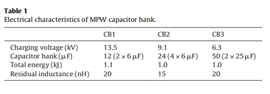
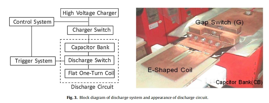
The block diagram of the discharge system is shown in Fig. 3 which is consisted of a capacitor bank (C) and a spark gap switch (G) with a one layer E-shaped flat coil. For optimizing the weld quality,three capacitor banks with different energy storage capacity were used in present experimental setup. The capacitor banks (CB) descriptions were summarized in Table 1. The capacitor bank is connected to the gap-switch and one-turn coil by a low inductance transmission line.
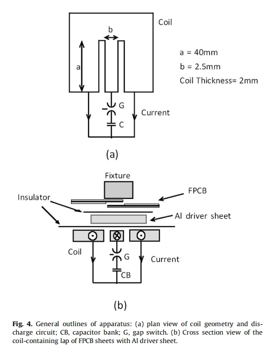
3.1. General outlines of apparatus
Fig. 4 shows the general outlines of the magnetic pulse welding apparatus. The coil was made by Cr–Cu alloy. The main discharge current pass through the middle part of coil and the width of this part was designed to be 2.5 mm and length of40 mm. The thickness of E-shaped coil was 2 mm and its inductance was measured about 0.039 μH. The thickness of Al driver was 0.3 mm with size of 50 mm × 50 mm. The skin depth for a typical discharge in this Al driver sheet was calculated by Eq. (2) and it was about 0.22 mm. This value is enough to prevent of melting of FPCB and apply big electromagnetic force to Al driver sheet for rapid collision with FPCB and producing a solid state boding.
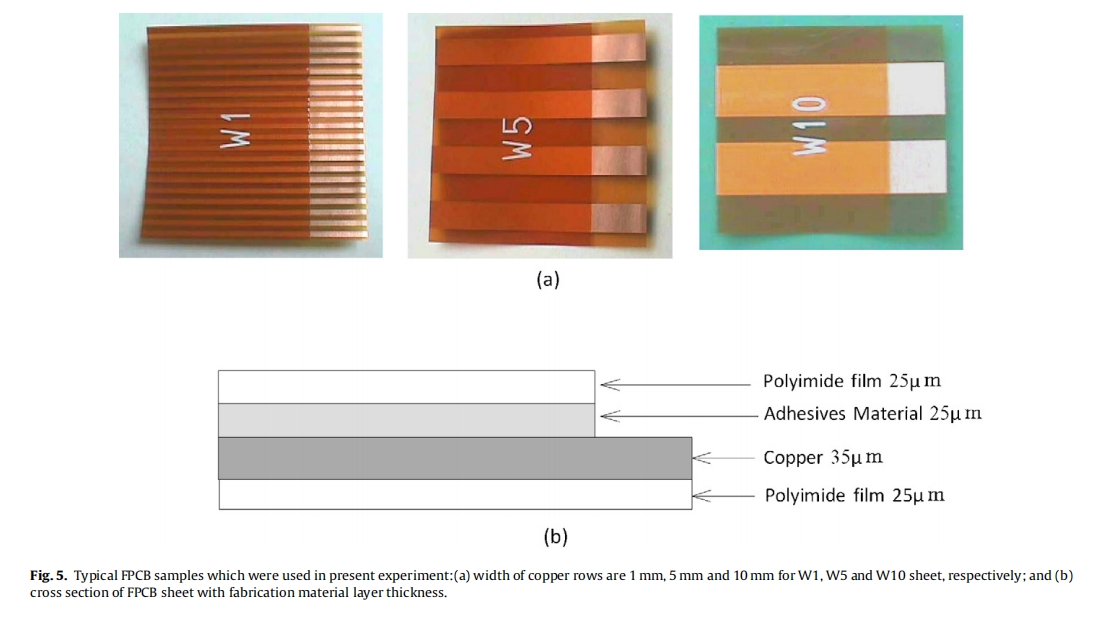
3.2. FPCB sample
A typical FPCB samples and its dimensional size which were used in present experiment are shown in Fig. 5a. Three types of FPCB sheet (W1, W5 and W10) which almost is used in industrial applications was chosen in present experiment. The size of FPCB sheet is 40 mm ×40 mm and the width of copper rows are 1 mm, 5 mm and 10 mm for W1, W5 and W10, respectively. The cross sec- tion view of all FPCB sheet layers are same and are shown in Fig. 5b. The total thickness ofFPCB is about 110 μm and the polyimide film layer cover only 30 mm of copper foil and 10 mm of that is uncoated (welding zone).